|
|
One of the fundamental problems dealing with Charge Coupled Device (CCD) detectors is to correct for the inefficiency of transferring charge through the device. The AXAF focal plane contains 10 CCDs of which 8 are front-illuminated (FI) devices and 2 are back-illuminated devices (see AXAF Observatory Guide). A brief description of ACIS CCDs can also be found in the Science Instrument (SI) Calibration Report for the AXAF CCD Imaging Spectrometer (ACIS), which we from now on refer to as the ACIS IPI report and recommend as a source of reference throughout this report. Each device is divided into two main sections, the image and framestore section. Charge is read out at four amplifier nodes leading to four independent read out units of 1026 rows in the imaging section, 1026 row in the framestore section and 256 columns. We refer to these as quadrants, where quadrant c0 corresponds to readout node A, c1 to node B, c2 to node C, and c3 to node D.
All CCD detectors suffer from an inefficiency of transferring charge though the image and framestore sections of the device. This Charge Transfer Inefficiency (CTI) can be quantified to first order as the average fractional charge loss per pixel. What specifically causes CTI is yet poorly understood. Gendreau et al. 1995 describe the effect as a result from traps due to proton induced displacements in the silicon lattice (see also references therein). When X-ray photons hit the silicon layer electron charge packets are generated by photoelectric interaction of the X-ray photon with the lattice. When clocked out these charge packages pass charge traps loosing parts of their charge. Once filled any passing charge packet will not loose charge until the trap is emptied. While trapping timescales are extremely low (< 10^-7 s), detrapping times are of the order of several hundred milliseconds. Figure 9 in Gendreau et al. 1995 shows a temperature dependence of detrapping times of the order of 1 sec for temperatures below 170 K, which is above the operating temperature of 156 K. Quite unknown is the actual size and distribution of charge traps, which should be an individual characteristic of each quadrant. The size could also be a function of temperature (G. Prigozhin, priv. comm.) as well as position in the device. In general this all means that the assumption of an average fractional charge loss per pixel is only a crude measure of CTI, not taking in account a variety of non-linear effects.
It is also clear that because of their fundamentally different design (see ACIS IPI report), front- and back-illuminated devices have different levels of intitial CTI. In FI devices the initial level of CTI is of the order of 10^-7 s, for the BI device about a factor 100 higher. Initial here means without any degradation effects due to radiation damage as expected during on-orbit operations. The level in FI devices predicts charge loss effects far below 1% and initially should not affect the data. In BI devices the charge lost throughout the device will be already of the order of 2% and higher (based on 2052 transfers) and thus of immediate interest.
Extensive calibration measurements were performed at the MIT Center for Space Research Those measurements were designed to determine of the energy-to-pulse-height relationship, spectral resolution, and other dependencies of the response function as a function of instrument parameters such as temperature, detector clock levels, and readout mode (Bautz et al. 1997). A detailed description of the various measurements can be found in the ACIS CCD Subassembly Calibration Plan (DN 36-01323, Rev. A) issued by the ACIS IPI team. Each flight CCD was illuminated at 15 X-ray energies. Unfortunately the X-ray sources were not entirely monochromatic and suffered from a variety of impurities and the data have to be properly filtered by pulse height. Table 1 shows a list of the X-ray sources with the corresponding line energies, total accumulated counts per energy and device quadrant, and the approximate exposure time. The measurements are exclusively in flat field mode and were designed to determine the energy scale with an error less than 0.1%. Although most measurements were not designed to test spatial dependencies to a high accuracy, the statistics allows us in most cases to determine the centroid of a line in a 16x16 detection cell with better than 5% accuracy. Count rates did not vary throughout each measurement and were low enough that only single photons were counted. Therefore one has to keep in mind that the here determined CTI values correspond to a single flux level only and are not affected by any pileup effects. Temperature as well as frame time were kept at -120+-3 degrees C and 3.3 seconds respectively.
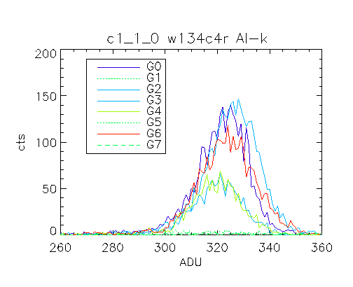
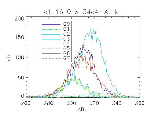
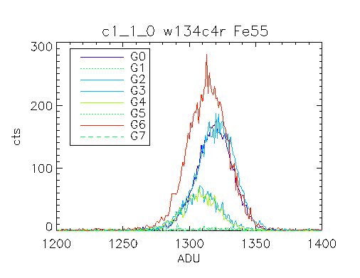
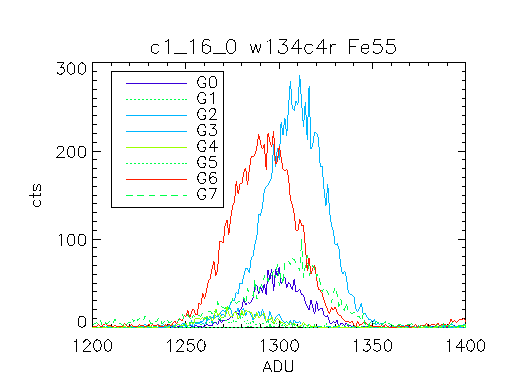
The data are affected by CTI in a variety of ways. To first instance CTI will lower the detected pulse height channel. Since charge is lost at each pixel-to-pixel transfer, events that are recorded far from the read-out node will have a lower detect pulse height channel than those detected near the read-out node. Figure 1 and figure 2 show the measured pulse heights for an Al-k source integrated over a 64x64 pixel detection cell. The different colors correspond to different grades (Note: all grades in this report given in ASCA grades). Figure 1 shows the pulse heights at the nearest corner of the image section to the readout node position, figure 2 the farthest corner. The shift to lower pulse heights in figure 2 is quite obvious and in this case (averaged over all grades) of the order of 20 ADU ($\sim$ 90 eV). CTI also causes grade migration, i.e. an initially graded event changes its grade during the transfer or gets completely lost. There may be two ways to consider the effect of grade migration, through charge tails and lost split events. In the case of charge tails it may be that enough charge is left behind in transfer direction that by the time it is read-out, it looks like split event. Charge tails may extend beyond the 3x3 or 5x5 event island in which case the charge is lost. In the case of the lost split it is possible that if an event is truly split between two pixels it may lose enough charge to fall below the split threshold and may look like a single pixel event. Figure 3 and figure 4 show the measured pulse heights for the Fe55 source integrated over a 64x64 pixel detection cell. The colors for the ASCA grades and positions on the device are the same as in Figure 1 and figure 2. It clearly can be seen that besides the expected pulse height shift the intensity as well as the positions of especially grades 1 (dark blue), 2 (light blue strong peak), and 6 (red) are quite different. Considering these effects it is quite conceivable that CTI also degrades energy resolution. This will happen in two ways. First, quite obvious, because charge is physically lost. Second, throughout the transfer noise is added to the data which results in a now spatial dependence of energy resolution. The latter effect is indicated in the grade 6 peak (red) in Figure 3 and figure 4. In order to practically quantify the CTI effects in form of an analytical function, we assume three different terms. In 0th order, i.e. a perfect world, there is only a very low constant inefficiency inherent to the device (C_{f,0}). A first order term (C_{f,1}), which is an average fractional charge loss per pixel across the entire device and may differ in energy and time, probably introduced by displacement induced traps or additional manufacturing procedures as it is the case for the back-illuminated devices. And a second order term containing all the non-linear residuals ((C_{f,2}), depending on energy, time, location on the device and event grade:
C_f(t) = C_{f,0} + C_{f,1}(E,t) + C_{f,2}(E,t,x,y,G).
The index f indicates that CTI is generally flux dependent. The time dependence of the first and second term is due to the expected on-orbit degradation due to radiation damage. The first two terms describe global effect on the device and a possible correction can be applied by using a generic algorithm on each event. The second term is a local one and may be applied as a second order correction matrix of certain custom grade sets. In the following we restrict ourselves to the first two terms:
C_f(t_0) = C_{f,0} + C_{f,1}(E,t_0),
where t_0 denotes the time before on-orbit radiation damage takes place.
Since the subassembly data allow us to determine CTI for a single flux level only, we will reduce the denomination of CTI from C_f(t_0) to only C in the following assessment. We need to measure CTI as the fraction of charge lost per pixel transfer. Transfer occurs in two modes on the device according to the two clocking directions, a parallel transfer of all pixels along columns (y-direction) through the image and frame store sections followed by a serial read-out across the columns (x-direction) at the corresponding node. This results in a serial CTI (C_s) and a parallel CTI (C_p) value. Since the data are taken in a flat field configuration the pulse height (PHA) versus pixel location can be directly fitted by a straight line:
y (or x) = b + m \times PHA
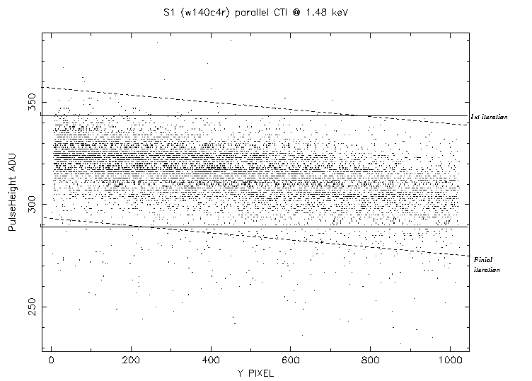
In order to separate the two directions it is necessary to select events nearest to the output node in each direction. We also have to minimize the effects of CTI in orthogonal directions but still maintain good statistics. Therefore we chose a window size for the serial CTI calculation to be 64 rows per node, and for the parallel CTI calculation 32 columns per node. Figure 5 shows an example of a pulse height versus pixel location in the parallel transfer direction for single pixel events. For each selected events a spectrum is computed and fit by a Gaussian function to get an estimate of the center pulse height channel. The rather low statistics in each data point allows quite a range of scatter in pulse height centroids. We then search for the center pulse height and select events within $\pm 5\sigma$ and adjust for the slope of the data and fit with a straight line. The slope has to be adjusted several times in order for the fit to converge. The CTI is then given by: C = {-m \over b}, $$ where the minus sign was introduced because CTI cannot be negative.
Front-illuminated Devices (FI)
Any type of CCD shows CTI effects as described above. However it is at some point relevant to define the actual calibration goal. If we want to achieve high spatial spectral linearity it is a reasonable assumption to tolerate a charge loss of the order of 1%. This means that for 2050 transfers the average fractional a CTI of the order of 5x10^{-6} or less can be considered as negligible. During MIT Lincoln Laboratory screening tests on all flight front side devices resulted in CTI estimates that clearly meet that criterium. Unfortunately those data are only available for the old flexed devices (after the tests were performed many of the selected flight devices had to be equipped with a new flexprint design). However, there is no reason to assume that CTI changed by more than a factor of 10 during the reflexing process. Table 2 therefore shows the screening results for the 8 flight FI devices for low (O-k, 525 eV) and high (Fe55, 5989 eV) energies. The values are averages over the four quadrant. Sometimes the screening resulted in a negative value and was excluded from the computation.
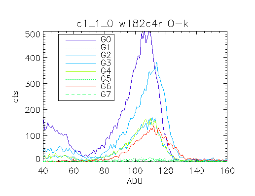
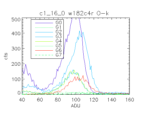
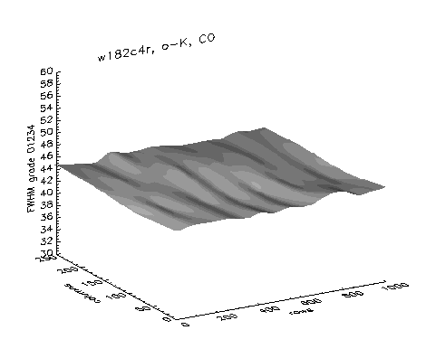
In order to investigate effects on pulse heights and spectral resolution in the spatial domain we analysed Al-k data of device w182c4r as a representative for all front side devices in more detail. Figure 6 and figure 7 show the pulse heights for the measured O-k line at the closest corner of the image section of quadrant 1 to the readout node and the farthest corner. The distribution of ASCA grades are again indicated by color. We used the O-k line because, as table 2 indicates, CTI is higher at low energies. The measured shift between the pulse heights amounts to 6 ADU. The grade distribution does not change indicating no apparent grade migration. This indicates a difference in pulse heights of the order of 2%. Figure 8 shows the spatial distribution of spectral resolution across quadrant 1. The smoothed spline grid was calculated from 64 spectral resolution data points generated across the quadrant using 64x64 pixel cells. No spatial degradation is visible throughout the quadrant indicating that no additional noise is introduced by CTI.
Table 3 shows the induced pulse height variations per quadrant for device w182c4r in parallel and serial direction. The values give the maximum number of ADUs observed throughout one single node. Each number is rounded towards its nearest integer. The values are measured for the standard grade set G02346.
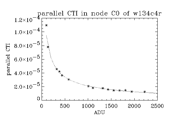
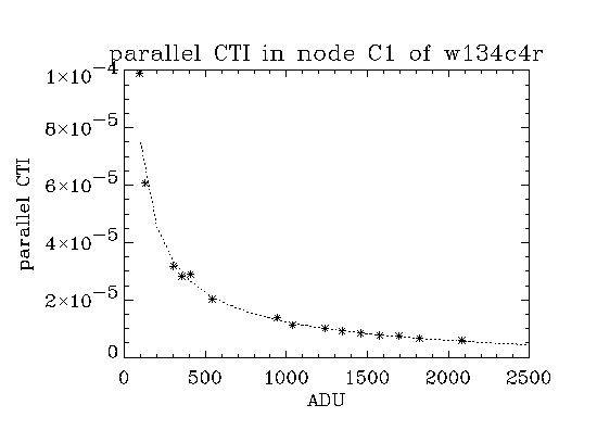
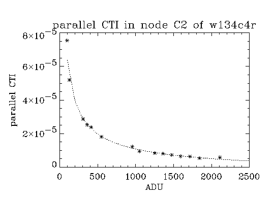
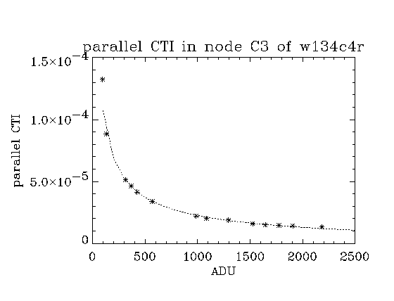
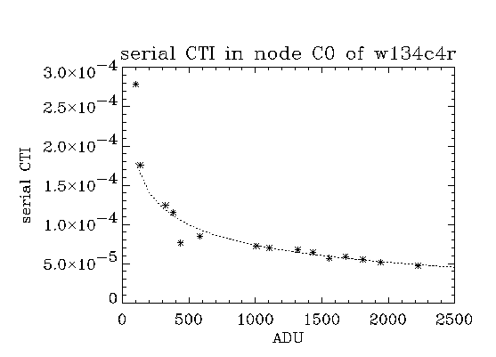
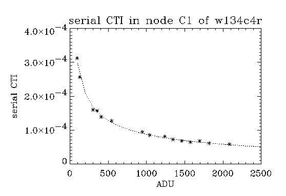
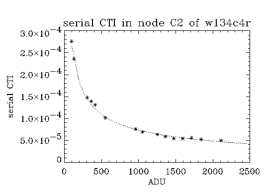
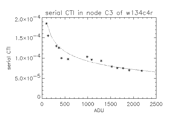
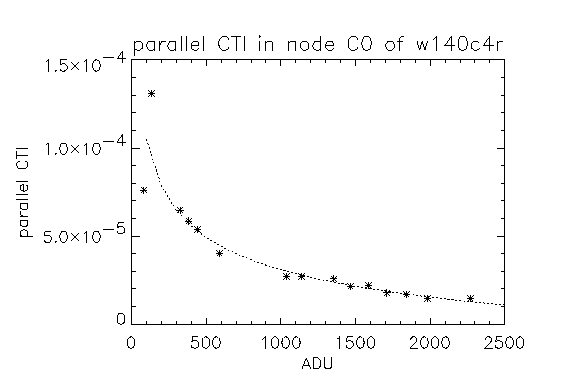
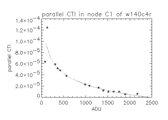
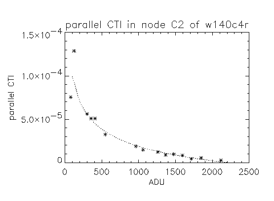
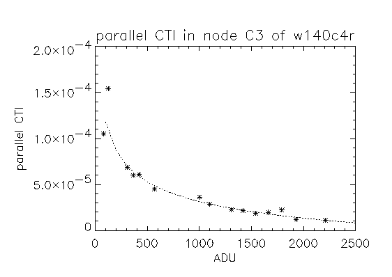
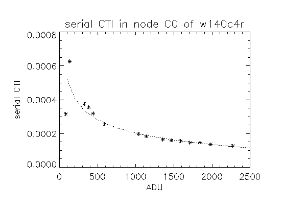
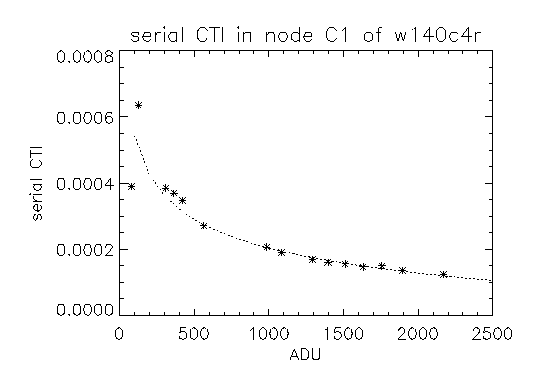
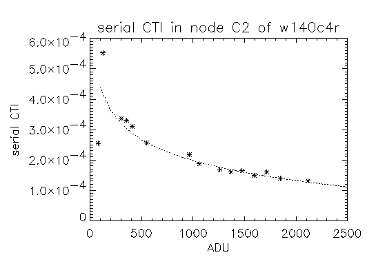
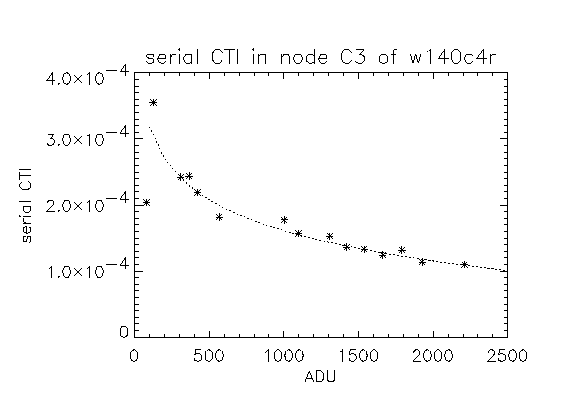
Because of some extended treatment during the manufacturing process back-illuminated devices show a higher affinity towards CTI effects. This became already a fact during Lincoln Lab screening of the old flexed devices, which indicated about a factor 100 higher charge loss per pixel transfer than observed in FI devices. It also appears that the two BI devices in the ACIS-S array themselves behave quite differently. The average FWHM versus energy in both devices, as specified in the ACIS IPI report, differ from 90 eV to 220 eV for w134c4r (S3) to 150 eV to 270 eV for w140c4r (S1) between 277 eV and 8029 eV respectively. In the following we therefore treat both BI CCDs as different devices.
We determined the average charge loss per pixel as described in section Determination of CTI for both BI devices in parallel and serial direction and fitted the result with a power law. In the following 2 sections we provide the result in from of plots, tables and fit coefficients. The energy dependence of both, parallel and serial, CTI values is well fit analytically by a power law. The fit is entirely empiric and its coefficients have no immediate physical meaning. However, those coefficients will come in quite handy, when we attempt do correct for the observed charge loss as well as when the here observed CTI is compared the one observed during the flat field measurements at XRCF.
The shift of pulse heights also affects the spectral resolution of the device. Besides the expected shift due to the shift in pulse heights, a significant increase in noise can be observed away from the read out nodes. A characterization of this effect can be found on the Spectral Resolution page.
w134c4r in S3 (FI)
w140c4r in S1 (FI)